
Home / Products / AI Vision Inspection & Ultrafast Laser Solutions
Our AI Vision Inspection & Ultrafast Laser Solutions help advanced manufacturers detect micro-defects, shorten production-line setup, and apply precise optical energy to demanding materials and imaging workflows. The portfolio combines configurable inspection hardware, deep-learning defect detection, and compact ultrashort-pulse laser technology for semiconductor, secondary-battery, display, precision-processing, and advanced-imaging applications.
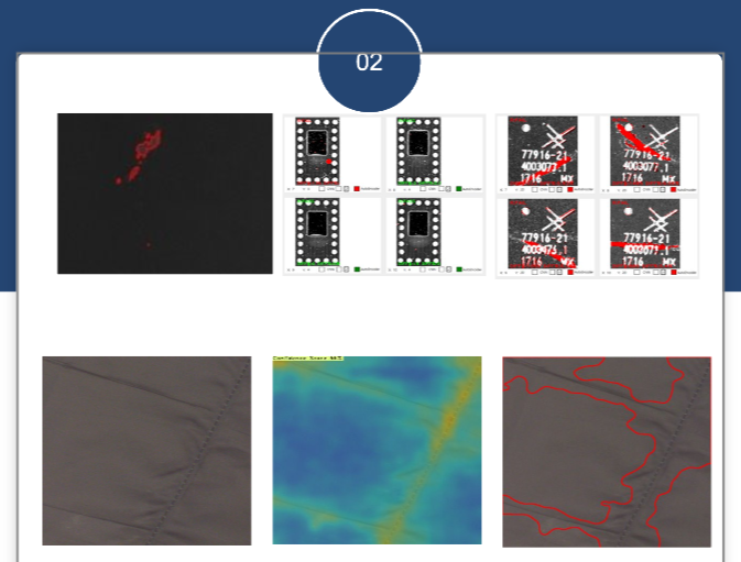
AI inspection combines production-ready optics with deep learning that can identify anomalies from normal-image training, reducing dependence on large predefined defect datasets.
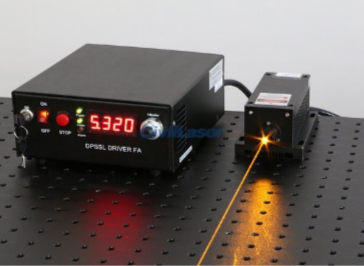
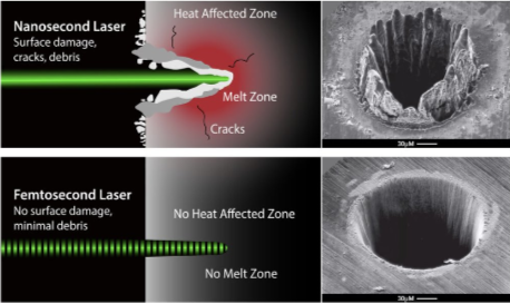
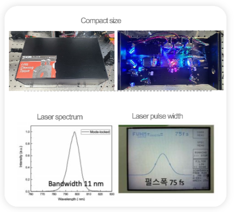
A compact ultrashort-pulse laser architecture supports high-precision processing and imaging with reduced thermal impact on surrounding material.

See how AI inspection and ultrafast optics bring speed, precision, and flexible configuration to advanced-manufacturing workflows.
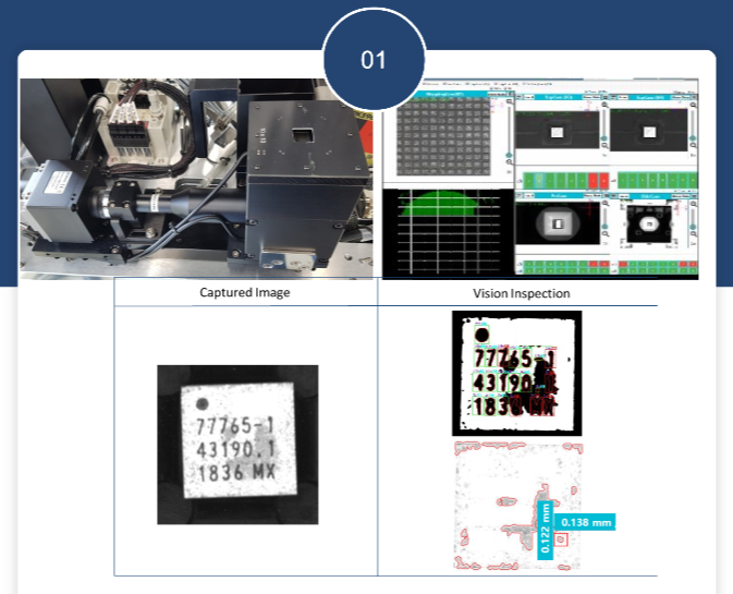
The deep-learning library can identify abnormal areas after training on normal images, reducing the need to collect and label every defect type in advance.
The source deck reports a 75% reduction in mass-production setup time, from eight weeks to two weeks, for its deep-learning inspection workflow.
On-the-fly vision inspection is listed at speeds up to 3 m/s, supporting in-line quality control without slowing the manufacturing flow.
Configurable optics and AI analysis support fine defect, position, dimension, pattern, and alignment inspection across semiconductor and battery processes.
Customized camera, lighting, and optical configurations can be designed around the surface, geometry, and defect characteristics of each application.
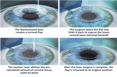
Compact femtosecond laser technology delivers short, high-peak-power pulses for precision processing and advanced imaging while limiting heat-affected zones.
“Modern production lines need more than a camera or a laser in isolation. They need inspection that learns quickly, optics tuned to the material, and precision energy delivered exactly where the process demands it. This portfolio brings those capabilities together for the next generation of manufacturing.”
See smaller defects. Set up faster. Process with precision.
Semiconductor packaging, secondary-battery production, and advanced displays are pushing inspection toward smaller defects, higher line speeds, and shorter setup cycles. At the same time, precision processing increasingly depends on ultrashort laser pulses that concentrate energy while limiting thermal damage. AI-based anomaly detection and compact femtosecond laser sources address these complementary quality and processing demands.
Smarter Quality Control, More Precise Processing
A dual-technology platform for demanding production environments.
Contact Us to Learn More About Our Capabilities
| Technology | Source-deck specification | Publication instruction |
|---|---|---|
| AI vision inspection | On-the-fly inspection up to 3 m/s; 97.6% inspection accuracy; customized optical systems | Confirm against the current model, material, defect definition, and acceptance test before publishing |
| Deep-learning library | Approx. 98% inspection accuracy; normal-image training; setup reduced from 8 weeks to 2 weeks | State the test dataset, benchmark, line conditions, and comparison basis before publishing |
| Ultrafast laser benchmark | 800 nm; >1,000 mW average power; <55 fs pulse duration; 68.8 MHz; ±0.5% rms stability; 264 kW peak power | The deck labels these as ETRI Laser values; confirm the commercial product configuration and current datasheet |
| Deployment proof | 300+ units; 12 mass-production sites; 7 countries | Revalidate the count and obtain permission before naming customers, countries, or sites |
| Configuration | Hardware listed in the source deck | System performance listed |
|---|---|---|
| Saw singulation vision | 6 cameras; 12 MP; 10 µm/pixel; 7-channel RGB low-angle and half-mirror lighting | PKG/ball/pattern <5 µm; alignment <5 µm; defect-detection threshold >50 µm |
| Loader / unloader vision | 5 cameras; 4/5 MP; 12 µm/pixel; 6-channel RB low-angle and half-mirror lighting | PKG/ball/pattern <6 µm; alignment <6 µm; defect-detection threshold >60 µm |
| Area | Website-ready application summary |
|---|---|
| AI vision inspection | Semiconductor package and alignment inspection; secondary-battery foil, chamfer, tab, marking, and dimensional inspection; and advanced-display defect inspection |
| Industrial laser | Battery laser notching, precision semiconductor processing, wafer dicing, and other low-thermal-impact processes |
| Advanced imaging | Two-photon and Raman imaging research, pathology imaging, and other precision optical applications |
Contact our team to discuss materials, line speed, defect types, optical configuration, laser requirements, system integration, validation, distribution opportunities, or a tailored demonstration.

Bridging Korean innovation with American business needs since 2010.